JUNE 25, 2024 by DGIST (Daegu Gyeongbuk Institute of Science and Technology)
Collected at: https://techxplore.com/news/2024-06-scientists-highly-efficient-technology-generation.html
DGIST’s Electrical Engineering and Computer Science Professor Jang Jae-eun and Professor Kwon Hyuk-jun and their research team have developed a high-efficiency process technology for next-generation AI memory transistors. The work is published online in Advanced Science.
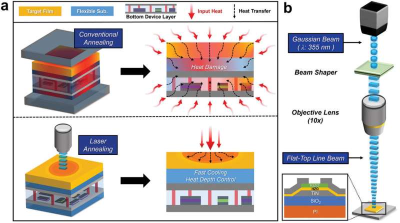
The team developed a nanosecond pulsed laser-based “selective heat treatment method” and “thermal energy minimization control process technology” to overcome the shortcomings of the high-temperature process of ferroelectric field-effect transistors, which have non-volatile memory characteristics, high-speed operation, low power consumption, long lifetime, and durability.
The new technology process enables the realization of heterojunction structures, which are the core technology of next-generation AI semiconductors.
As various electronic systems are developed in the Fourth Industrial Revolution, high-level information processing and storage technologies are in demand. Most of all, AI-type memory transistor technology, which performs computation and memory simultaneously, like the human brain, is an exceptional technology with advantages such as reduced manufacturing costs, power efficiency, high performance, lightweight, and improved integration, and in-depth research is being conducted in this field.
Recent research on AI-type memory transistors has been centered on ferroelectric field-effect transistors, which have non-volatile memory characteristics, high-speed operation, low power consumption, long lifetime, and durability.
However, due to the characteristics of ferroelectrics that require a “high-temperature phase formation process” (over 600 degrees Celsius), there is the issue that the characteristics of the transistors are degraded or thermal damage is caused to the lower layers of logic circuits or input/output (I/O) circuits when the heterojunction of memory devices is performed.
To overcome the shortcomings of ferroelectric processes, a joint research team led by DGIST Professors Jang Jae-eun and Kwon Hyuk-jun conducted research to develop heat treatment methods for specific parts and control process technology to minimize thermal energy. The team introduced a “nanosecond pulsed laser annealing process” that enables selective heat treatment to solve the problem of high-temperature processes.
The process has a short wavelength (355 nm), a penetration depth as thin as two-thousandths of a human hair, and fast cooling characteristics utilizing a pulsed laser in 30 millionths of a second, which is highly advantageous for controlling thermal energy and promoting ferroelectricity in ferroelectrics.
Using this technology, the team developed memory transistors with ferroelectrics and semiconductor channels that are active even at low temperatures and that have highly efficient AI semiconductor characteristics.
The optimized device has an ultra-fast response time of a millionth of a second, performing over 100,000 stable write and erase operations in an accelerated measurement environment and maintaining the memory state for over 10 years. In addition, the transistor has a “memory operating range” of over 1.7V, an on-off current ratio over 100,000, showing excellent power consumption performance and high ferroelectric properties (2-Pr of 14.7 µC/cm2) and pattern recognition linearity, as well as demonstrating outstanding mechanical, electrical, and chemical performance.
More information: Dongsu Kim et al, Low‐Temperature Nanosecond Laser Process of HZO‐IGZO FeFETs toward Monolithic 3D System on Chip Integration, Advanced Science (2024). DOI: 10.1002/advs.202401250
Journal information: Advanced Science
Leave a Reply