November 7, 2024 by Amy Walden, Florida State University
Collected at: https://phys.org/news/2024-11-physicists-reveal-layers-impact-graphene.html
When it comes to electrically conductive nanomaterials, graphene—stronger and lighter than steel and more conductive than copper—has been shown to be an excellent choice for a wide range of technologies.
Physicists are working to learn more about this impressive form of naturally occurring elemental carbon, which is composed of a single flat layer of carbon atoms arranged in a repeating hexagonal lattice.
Now, researchers from the Florida State University Department of Physics and FSU-headquartered National High Magnetic Field Laboratory have published findings that reveal how various physical manipulations of graphene, such as layering and twisting, impact its optical properties and conductivity. The study is published in the journal Nano Letters.
The team, led by Assistant Professor Guangxin Ni, along with Assistant Professor Cyprian Lewandowski and graduate research assistant Ty Wilson, found that the conductivity of twisted bilayer graphene is not heavily impacted by physical or chemical manipulations and instead depends more on how the material’s minute geometry structure changes by interlayer twisting—a revelation that opens the door for additional studies on how lower temperatures and frequencies impact graphene’s properties.
“This specific path of research began as an attempt to explain some of the optical properties of twisted bilayer graphene, as this material has been imaged with scanning near-field optical microscopes before, but not in a way that compared different twisting angles,” Wilson said. “We wanted to examine this material from that perspective.”
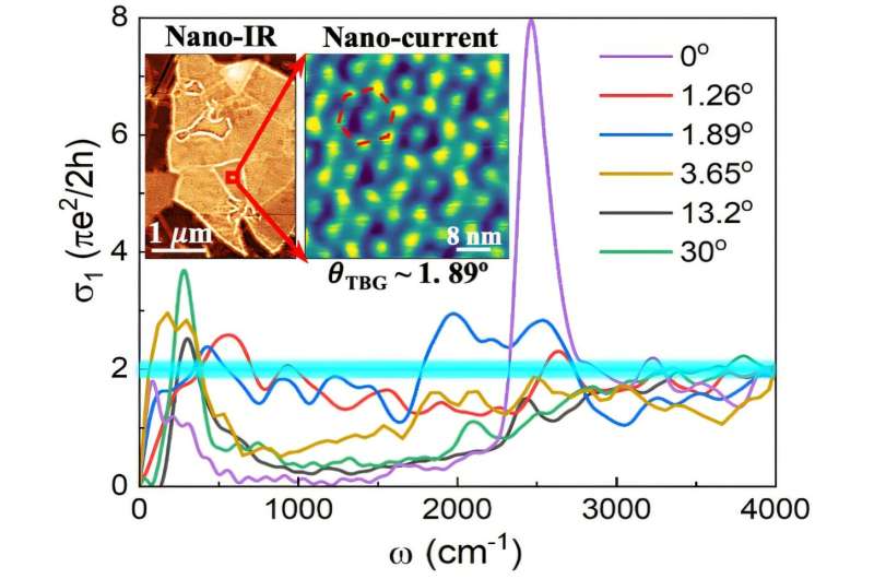
To conduct the study, the team captured images of plasmons—tiny waves of energy that happen when electrons in a material move together—that appeared in various regions of the twisted bilayer graphene.
“The scanning near-field optical microscope essentially shines a certain wavelength of infrared light onto the sample, and the scattered light is collected back to form a nanoscale image that is way below the diffraction limit,” Wilson said. “The key here is that it involves a needle that substantially boosts the light-matter coupling, enabling us to see these plasmons using nano-light.”
The team analyzed the grain boundaries, or defects in the crystal structure, in the resulting images to identify different regions of the twisted bilayer graphene. These regions containing the plasmons piqued the team’s interest because the two sheets of carbon atoms were twisted at discrete angles in each, in addition to themselves being twisted with respect to a layer of hexagonal boron nitride—a transparent layered crystal—placed underneath.
Physicists refer to the geometrical design that results when a set of straight or curved lines is superimposed onto another set as a moiré pattern, derived from a French word for “watered.” The twisting of the bilayer graphene and boron nitride resulted in the formation of what’s known as a double-moiré structure, two layers of patterns, also known as a superlattice.
“The plan was to compare the reflected near-field signal we got for each domain, whereas most previous research on graphene looked only at a single twist angle, and never before with these ‘moiré of moiré’ systems,” Wilson said.
The team found that the optical conductivity of twisted bilayer graphene with boron nitride does not vary much with twist angle for angles of less than two degrees, even when the graphene is electrically doped and exposed to changing frequencies of infrared light.
“What this tells us is the opto-electronic properties of this super-moiré material are independent of chemical doping or the twisted bilayer graphene’s twist angle, and instead depend more on the super-moiré structure itself and how it affects the electronic bands in the material, allowing for enhanced optical conductivity,” Wilson said.
Lewandowski added that this result is exciting because it highlights the potential of multilayer moiré systems in constructing materials with “on-demand” optical properties.
“The measurement technique used by Professor Ni’s group allows us to probe the local optical response of 2D systems, complementing other local measurement techniques commonly used for 2D materials,” he said. “Interestingly, in conjunction with accompanying theoretical modeling, the reported measurement argues how a 2D system can achieve almost uniform optical response over a wide light frequency range passively, without the need for active electronic feedback.”
The team’s findings indicate the significant impact of geometric relaxations in double-moiré lattices, which helps researchers to better understand how nanomaterials like graphene may respond to different manipulations. In turn, this information can be used to help scientists produce desirable optical properties—like enhanced conductivity—in a material, allowing for innovative advancements in moiré optoelectronics, including thermal imaging technologies and optical switching in computer processors.
“This paves the way for our continuous exploration of various nano-optical and electronic phenomena that are unattainable with alternative diffraction-limited far-field optics,” Ni said.
More information: Songbin Cui et al, Nanoscale Optical Conductivity Imaging of Double-Moiré Twisted Bilayer Graphene, Nano Letters (2024). DOI: 10.1021/acs.nanolett.4c02841
Journal information: Nano Letters

Leave a Reply