September 19, 2024 by Elizabeth A. Thomson, Materials Research Laboratory, Massachusetts Institute of Technology
Collected at: https://phys.org/news/2024-09-material-wavy-layers-atoms-unusual.html
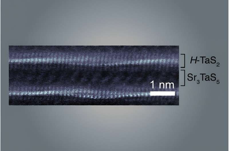
MIT physicists and colleagues have created a new material with unusual superconducting and metallic properties, thanks to wavy layers of atoms only billionths of a meter thick that repeat themselves over and over to create a macroscopic sample that can be manipulated by hand. The large size of the sample makes it much easier to explore its quantum behavior, or interactions at the atomic scale that give rise to its properties.
The work, reported in Nature, is also important because the material was synthesized through rational design. In other words, the recipe for the material is based on the team’s insights into the materials science and chemistry of this family of materials. As a result, the physicists are confident they can create even more new materials with unusual properties.
Further, although there are other materials that form wavy atomic structures, the team believes that this is the most perfect. The nanoscopic layers of waves are uniform across an entire crystal, which is composed of thousands of these corrugated layers.
“Such materials go beyond what one would conventionally consider a crystal—observing and understanding what new physical properties may emerge is an exciting opportunity,” says Joseph Checkelsky, senior investigator of the work and Associate Professor of Physics at MIT.
2D materials
Two-dimensional materials, or those consisting of only one or a few layers of atoms, have captured physicists’ attention because they can be manipulated to produce materials with new, unusual properties. For example, rotating, or twisting, one or more of the layers at a slight angle creates a unique pattern called a moiré superlattice that can give rise to phenomena including superconductivity and unconventional magnetism.
But moiré materials are both difficult to make—they must be assembled manually—and difficult to study because of their atomic dimensions. Checkelsky’s group has been working to create analogous materials that are much easier to manipulate.Play
“We essentially mix powders of material, expose them to temperatures of a few hundred degrees Celsius in a furnace, and rely on chemical reactions” to naturally form macroscopic crystals with properties dictated by atomic-scale interactions. “That’s the key breakthrough,” says Aravind Devarakonda, MIT Ph.D., who is now an assistant professor at Columbia University. Devarakonda is first author of the current Nature paper.
In 2020, Checkelsky and many of the same colleagues in the current work reported the first such material created this way in the journal Science. That paper was accompanied by a perspective piece by Professor Leslie M. Schoop of Princeton University.
In 2021, Checkelsky and colleagues described in Nature the physics behind how that particular material can exhibit two different kinds of superconductivity. The new wavy material is the second member of this family of compounds.
Like a layer cake
Like a layer cake, the new material is composed of an atomically thin metallic layer of tantalum and sulfur stacked on top of a “spacer” layer composed of strontium, tantalum, and sulfur. This structure repeats over thousands of layers to create a large crystal.
Devarakonda and colleagues believe the waves form due to a mismatch in the size and structure of each layer’s crystal lattice. Correspondingly, one layer—composed of tantalum and sulfur—buckles to fit atop the other, forming the wave. Imagine placing a sheet of legal paper over a sheet of regular printer paper. For the legal paper to fit atop the regular paper, some of the paper would need to buckle upward. The new structure is analogous, except that the legal paper is “pinned” to the regular paper at intervals, forming waves.
Unusual properties
Those minuscule waves, in turn, are behind the material’s interesting properties. For example, at a certain temperature the material can become superconducting, where electrons travel through a material with no resistance.
In this case, “the electrons are imprinted by the structural modulations [waves],” Devarakonda says. In other words, “the superconductivity also picks up this waviness. In some parts it is strong, and in other parts it’s weakened.”
Similarly, the material has unusual metallic properties. That’s because electrons find it much easier to flow down the troughs of a wave—or down a valley—as opposed to up and over the hills of a wave.
“So what we’ve done is given the electrons a directionality. It’s easier for them to flow in one direction versus the other,” Devarakonda says. “We’ve shown that by introducing the [wave] structure we can drastically change the behavior of the layers. We’ve planted the flag; now we and others can run with applications. By standing on the shoulders of giants, we’ve created an entirely new family of materials. It’s completely uncharted territory that has brought unexpected outcomes, and surprises are always fun.”
In addition to Devarakonda and Checkelsky, authors of this paper are Alan Chen, a graduate student in MIT’s Department of Electrical Engineering and Computer Science; Shiang Fang, formerly a postdoctoral researcher in MIT’s Department of Physics, now at Google Deepmind; David Graf of the National High Magnetic Field Laboratory; Markus Kriener of the RIKEN Center for Emergent Matter Science in Japan; Austin J. Akey of Harvard University; David C. Bell of Harvard; and Takehito Suzuki of Toho University.
More information: A. Devarakonda et al, Evidence of striped electronic phases in a structurally modulated superlattice, Nature (2024). DOI: 10.1038/s41586-024-07589-5

Leave a Reply