August 5, 2024 by KeAi Communications Co.
Collected at: https://techxplore.com/news/2024-08-micro-oled-technology-20k-ppi.html
From OLED displays to programmable lighting and biosensors, organic semiconductors have found increasing applications since thin-film devices were first reported in the 1980s. Recently, the rapid development of wearable electronics has driven the evolution towards ever-higher device resolutions, enabling immersive experiences in near-eye displays like virtual and augmented reality devices.
In a review published in the journal Wearable Electronics, scientists from Germany and China summarized their systematic work in developing a photolithography-compatible technology for the fabrication of ultra-high-resolution organic semiconductor devices.
“For inorganic semiconductors like silicon, device dimensions are approaching 1 nm using well-developed photolithographic technology, enabling the integration of 200 million transistors in an area of just one square millimeter,” explains Wenchong Wang, a senior scientist at the University of Muenster.
“Unfortunately, due to the deterioration caused by UV light and solvents to organic materials, photolithography technology cannot be simply applied. Alternative patterning methods, like fine metal masks, have resolutions of only tens of micrometers, limiting the number of devices on a square millimeter to hundreds.”
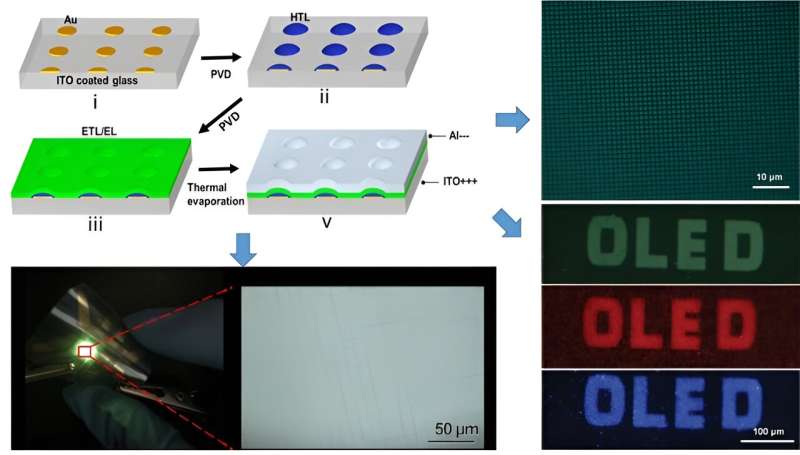
Given the potential for ultra-high resolution, photolithography would be an ideal patterning method for organic materials if it could be performed without damaging their functionalities. The researchers addressed this challenge by introducing the strategy of “first surface patterning and then patterned growth.”
What this means is that the substrate surface was first patterned by lithography before organic materials were introduced. Subsequently, organic semiconductor molecules were deposited, allowing them to diffuse on the surface and selectively grown at designated areas, resulting in pattern formation and device fabrication on substrates.
As a result, OLEDs with resolutions of over 20K ppi were achieved, meeting the requirements for next-generation displays.
“Our approach avoids the damage caused by lithographic procedures to organic semiconductors, offering significant advantages in terms of surface engineering and device resolution,” noted Lifeng Chi, the study’s lead investigator and professor at Soochow University.
“Future wearable electronics will require monolithic integration of multifunctional systems on a chip, including information collection, transmission, processing, storage, and display. Together with our collaborators, we are working towards even more advanced and compact devices.”
More information: Wenchong Wang et al, Patterned growth of organic semiconductors for ultra-high resolution microelectronics and optoelectronics, Wearable Electronics (2024). DOI: 10.1016/j.wees.2024.05.005

Leave a Reply