26 Nov 2024 Isabelle Dumé
Collected at: https://physicsworld.com/a/electromagnetic-waves-solve-partial-differential-equations/
Waveguide-based structures can solve partial differential equations by mimicking elements in standard electronic circuits. This novel approach, developed by researchers at Newcastle University in the UK, could boost efforts to use analogue computers to investigate complex mathematical problems.
Many physical phenomena – including heat transfer, fluid flow and electromagnetic wave propagation, to name just three – can be described using partial differential equations (PDEs). Apart from a few simple cases, these equations are hard to solve analytically, and sometimes even impossible. Mathematicians have developed numerical techniques such as finite difference or finite-element methods to solve more complex PDEs. However, these numerical techniques require a lot of conventional computing power, even after using methods such as mesh refinement and parallelization to reduce calculation time.
Alternatives to numerical computing
To address this, researchers have been investigating alternatives to numerical computing. One possibility is electromagnetic (EM)-based analogue computing, where calculations are performed by controlling the propagation of EM signals through a materials-based processor. These processors are typically made up of optical elements such as Bragg gratings, diffractive networks and interferometers as well as optical metamaterials, and the systems that use them are termed “metatronic” by analogy with more familiar electronic circuit elements.
The advantage of such systems is that because they use EM waves, computing can take place literally at light speeds within the processors. Systems of this type have previously been used to solve ordinary differential equations, and to perform operations such as integration, differentiation and matrix multiplication.
Some mathematical operations can also be computed with electronic systems – for example, with grid-like arrays of “lumped” circuit elements (that is, components such as resistors, inductors and capacitors that produce a predictable output from a given input). Importantly, these grids can emulate the mesh elements that feature in the finite-element method of solving various types of PDEs numerically.
Recently, researchers demonstrated that this emulation principle also applies to photonic computing systems. They did this using the splitting and superposition of EM signals within an engineered network of dielectric waveguide junctions known as photonic Kirchhoff nodes. At these nodes, a combination of photonics structures, such as ring resonators and X-junctions, can similarly imitate lumped circuit elements.
Interconnected metatronic elements
In the latest work, Victor Pacheco-Peña of Newcastle’s School of Mathematics, Statistics and Physics and colleagues showed that such waveguide-based structures can be used to calculate solutions to PDEs that take the form of the Helmholtz equation ∇2f(x,y)+k2f(x,y)=0. This equation is used to model many physical processes, including the propagation, scattering and diffraction of light and sound as well as the interactions of light and sound with resonators.
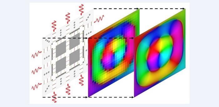
Unlike in previous setups, however, Pacheco-Peña’s team exploited a grid-like network of parallel plate waveguides filled with dielectric materials. This structure behaves like a network of interconnected T-circuits, or metatronic elements, with the waveguide junctions acting as sampling points for the PDE solution, Pacheco-Peña explains. “By carefully manipulating the impedances of the metatronic circuits connecting these points, we can fully control the parameters of the PDE to be solved,” he says.
The researchers used this structure to solve various boundary value problems by inputting signals to the network edges. Such problems frequently crop up in situations where information from the edges of a structure is used to infer details of physical processes in other regions in it. For example, by measuring the electric potential at the edge of a semiconductor, one can calculate the distribution of electric potential near its centre.
Pacheco-Peña says the new technique can be applied to “open” boundary problems, such as calculating how light focuses and scatters, as well as “closed” ones, like sound waves reflecting within a room. However, he acknowledges that the method is not yet perfect because some undesired reflections at the boundary of the waveguide network distort the calculated PDE solution. “We have identified the origin of these reflections and proposed a method to reduce them,” he says.
In this work, which is detailed in Advanced Photonics Nexus, the researchers numerically simulated the PDE solving scheme at microwave frequencies. In the next stages of their work, they aim to extend their technique to higher frequency ranges. “Previous works have demonstrated metatronic elements working in these frequency ranges, so we believe this should be possible,” Pacheco-Peña tells Physics World. “This might also allow the waveguide-based structure to be integrated with silicon photonics or plasmonic devices.”

Leave a Reply