September 16, 2024 by David Bradley, Inderscience
Collected at: https://techxplore.com/news/2024-09-semiconductor-refined-algorithm-wafer-defects.html
Research published in the International Journal of Information and Communication Technology may soon help solve a long-standing challenge in semiconductor manufacture: the accurate detection of surface defects on silicon wafers. Crystalline silicon is the critical material used in the production of integrated circuits and in order to provide the computing power for everyday electronics and advanced automotive systems needs to be as pristine as possible prior to printing of the microscopic features of the circuit on the silicon surface.
Of course, no manufacturing technology is perfect and the intricate process of fabricating semiconductor chips inevitably leads to some defects on the silicon wafers. This reduces the number of working chips in a batch and leads to a small, but significant proportion of the production line output failing.
The usual way to spot defects on silicon wafers has been done manually, with human operators examining each wafer by eye. This is both time-consuming and error-prone due to the fine attention to detail required. As wafer production has ramped up globally to meet demand and the defects themselves have become harder to detect by eye, the limitations of this approach have become more apparent.
Chen Tang, Lijie Yin and Yongchao Xie of the Hunan Railway Professional Technology College in Zhuzhou, Hunan Province, China explain that automated detection systems have emerged as a possible solution. These too present efficiency and accuracy issues in large-scale production environments. As such, the team has turned to deep learning, particularly convolutional neural networks (CNNs), to improve wafer defect detection.
The researchers explain that CNNs have demonstrated significant potential in image recognition. They have now demonstrated that this can be used to identify minute irregularities on the surface of a silicon wafer. The “You Only Look Once” series of object detection algorithms is well known for being able to balances accuracy against detection speed.
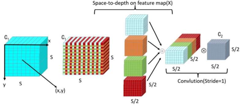
The Hunan team has taken the YOLOv7 algorithm a step further to address the specific problems faced in wafer defect detection. The main innovation in the work lies in using SPD-Conv, a specialized convolutional operation to enhance the ability of the algorithm to extract fine details from images of silicon wafers. Additionally, the researchers incorporated a Convolutional Block Attention Module (CBAM) into the model to sharpen the system’s focus on smaller defects that are often missed in manual inspection or by other algorithms.
When tested on the standard dataset (WM-811k) for assessing wafer defect detection systems, the team’s refined YOLOv7 algorithm achieved a mean average precision of 92.5% and had a recall rate of 94.1%. It did this quickly, at a rate of 136 images per second, which is faster than earlier systems.
More information: Chen Tang et al, Wafer surface defect detection with enhanced YOLOv7, International Journal of Information and Communication Technology (2024). DOI: 10.1504/IJICT.2024.141433

Leave a Reply