By Nagoya University September 13, 2024
Collected at: https://scitechdaily.com/powering-the-tech-of-tomorrow-metal-nanowire-mass-production-breakthrough/
A new technique for growing metal nanowires promises to transform electronics manufacturing.
By increasing the density of aluminum nanowires significantly, this method maintains high purity and could be applied to other metals, enhancing the production of advanced electronic components.
Nanowire Technology Breakthrough
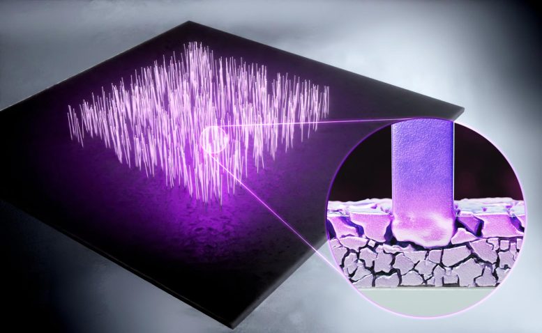
A research group from Nagoya University in Japan has created a new technique for growing the tiny metal nanowires (NWs) that are expected to be used in next-generation electronics. Their results suggest a way to mass produce pure metal NWs, which has until now limited their use. The new technique promises to enhance the efficiency of electronics production, including circuitry, LEDs, and solar cells. The study was published recently in the journal Science.
Mass production of NWs has been challenging because of the difficulties of scaling production while maintaining quality and purity. NWs are so small that they are made by transporting atoms, the smallest constituent of matter, typically in a gas phase state. However, that is difficult to do with metals, hindering the production of these important components of electronics.
Innovative Growth Technique
To overcome this problem, a group led by Yasuhiro Kimura at the Nagoya University Graduate School of Engineering used atomic diffusion in a solid phase state enhanced by ion beam irradiation to create aluminum NWs from single crystals.
Atomic diffusion is a process by which atoms or molecules move from areas of high concentration to areas of low concentration, through stress state change under heat. Using ion beams, the crystal grains were irradiated inside the thin aluminum film to coarsen them at the surface layer. This caused changes in stress distribution, guiding atomic flow, and was used as a means of supplying mass atomic feedstocks for NW growth to specific locations. In practice, when heat was applied, there was an upward flow of atoms through the gradient from the fine grains on the bottom to the coarse ones on top, resulting in mass growth of NWs.
Breakthrough in Nanowire Density
“We increased the density of aluminum NWs from 2×10⁵ NWs per square cm to 180×105 per square cm,” Kimura said. “This achievement paves the way for bottom-up metal NW growth methods, which have so far been grown only accidentally and in small quantities. It can also be extended to other metals in principle.”
Potential Applications and Future Outlook
The resulting aluminum NWs are expected to be utilized as nanocomponents for sensing devices and optoelectronics due to their unique features, such as a large surface area, good mechanical properties derived from being made from single crystals, and their resistance to natural oxidation.
“We realized mass growth of forest-like metallic NWs using only three key processes: thin film deposition on a substrate, ion beam irradiation, and heating,” Kimura explained. “Our technique solves the urgent need to establish mass production methods, especially in the production of high-performance nanodevices such as gas sensors, biomarkers, and optoelectronic components.”
Reference: “Growth of metal nanowire forests controlled through stress fields induced by grain gradients” by Yasuhiro Kimura, Yi Cui, Takamasa Suzuki, Yuki Tanaka, Takaaki Tanaka, Yuhki Toku and Yang Ju, 8 August 2024, Science.
DOI: 10.1126/science.adn9181
Leave a Reply