September 13, 2024 by National Research Council of Science and Technology
Collected at: https://techxplore.com/news/2024-09-p-semiconductor-materials-gen-displays.html
A group of Korean researchers have recently succeeded in developing new p-type semiconductor materials and thin-film transistors that will lead the innovation of the semiconductor industry. These new discoveries are expected to be widely utilized to improve the overall performance of next-gen displays and ultra-low power semiconductor devices.
Electronics and Telecommunications Research Institute (ETRI) has successfully developed a p-type Se-Te (Selenium-Tellurium) alloy transistor that can be easily deposited at room temperature via a simple process using a chalcogenide-based p-type semiconductor material. In addition, they have also developed a new technology that can systematically adjust and control the threshold voltage of n-type transistors through charge injection control of Te thin films in the heterojunction structure of n-type oxide semiconductor and p-type Te.
The work is published in the journal ACS Applied Materials & Interfaces.
Semiconductors are normally classified into intrinsic semiconductors and extrinsic semiconductors depending on their “doping status.” In other words, intrinsic semiconductors are ‘pure’ semiconductors without added impurities. In the case of silicones, which is a commonly used material in the semiconductor industry, no electrons can move within pure silicone, meaning no current flows even when a voltage is applied.
Therefore, specific impurities are added to the intrinsic semiconductor to utilize the characteristics of the semiconductor and electrical conductivity of the materials. Extrinsic semiconductors are divided into n-type semiconductors and p-type semiconductors according to the type of impurities added in the production/manufacturing process.
One of the most widely used materials in the current display industry is the IGZO(Indium Gallium Zinc Oxide)-based n-type oxide semiconductor. In the case of p-type semiconductors, p-type LTPS (Low-Temperature Polycrystalline Silicon) is used due to the lack of processability and electrical properties compared to n-type oxide semiconductors, but there has always been many limitations in that it is much more expensive to manufacture and the size of the substrate is limited.
However, with the increase in demand for higher refresh rates (240Hz+) in high-res displays, especially at SHV-class resolution displays (8K*4K), interest towards the development of p-type semiconductors has reached its peak in recent years. Since n-type semiconductor-based transistors, which have been used in existing displays, have limitations in effectively implementing displays with high refresh rates, demands for p-type semiconductors are increasing at a rapid pace.
To meet these needs, the researchers at ETRI succeeded in developing a p-type semiconductor by adding Te to Se, increasing the crystallization temperature of the channel layer, depositing an amorphous thin film at room temperature and crystallizing it through a subsequent heat treatment process. As a result, they have successfully secured improved mobility and a higher level of on/offline current ratio characteristics compared to existing transistors.
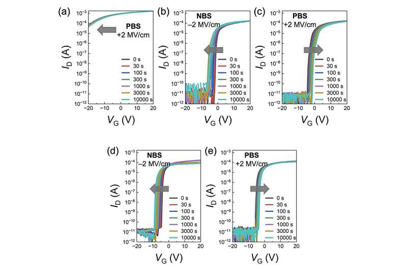
The researchers have also confirmed that when a Te-based p-type semiconductor was introduced as a heterojunction structure over an n-type oxide semiconductor thin film, the threshold voltage of the n-type transistor can be adjusted by controlling the flow of electrons within the n-type transistor depending on the thickness of Te. In particular, they have improved the stability of the n-type transistor without the need of a passivation layer, by adjusting thickness of Te in the heterojunction structure.
By utilizing these achievements, it is expected that the growth of next-gen display industry will reach new heights, enabling the development of new displays with better resolution and lower power consumption at the same time.
In fact, this new discovery can not only make meaningful contributions in the field of display, but it can also change the scenery of the semiconductor industry. Currently, many leading global semiconductor manufacturers are focusing on the development of new scale-down processes that can increase the integration of their products, but according to the analysis of many industry insiders, the level of integration in semiconductors has reached its limit.
Accordingly, in recent years, a new integration method has been introduced to stack multiple semiconductor chips at once. Among them, TSV (Through Silicon Vias) is the most well-known method, where multiple wafers are stacked and a hole is drilled into the wafers to ensure electrical connection. This TSV method has the advantage of effective utilization of space and reduced power consumption. However, there are still many limitations that need to be addressed, including high process costs, low yield, etc.
In fact, to overcome such limitations of TSV, the industry has come up with a new approach, also known as the Monolithic 3-dimensional (M3D) integration, where the materials are stacked onto a single wafer instead of stacking multiple layers at once. Unfortunately, the M3D method has not yet reached its commercialization stage due to various issues such as the limited use of high-temperature processes, etc.
However, many experts view that the heterojunction thin film transistor and p-type semiconductor device developed by ETRI can operate stably even in processes below 300℃, pushing the industry a step closer to the successful commercialization of M3D.
Cho Sung-Haeng, the Principal Researcher of ETRI’s Flexible Electronics Research Section, stated, “This is a monumental achievement that can be widely utilized in next-gen displays such as OLED TVs and XR devices, as well as future researchers in other fields such as CMOS (Complementary Metal Oxide Semiconductor) circuits and DRAM memories.”
Researchers of ETRI stated that they are planning to optimize the Te-based p-type semiconductors to large-sized substrates of 6 inches or larger and secure its potential for commercialization by applying them to various circuits, ultimately finding new ways to implement them into new fields.
More information: Jung Hoon Han et al, Tuning the Threshold Voltage of an Oxide Thin-Film Transistor by Electron Injection Control Using a p−n Semiconductor Heterojunction Structure, ACS Applied Materials & Interfaces (2024). DOI: 10.1021/acsami.4c02681
Journal information: ACS Applied Materials and Interfaces

Leave a Reply