August 21, 2024 by Ingrid Fadelli , Tech Xplore
Collected at: https://techxplore.com/news/2024-08-tensor-processor-chip-based-carbon.html
Artificial intelligence (AI) and machine learning tools have proved to be highly effective in tackling various tasks that entail analyzing data and making accurate predictions. Despite their advantages, these tools have significant computational demands, and when running on existing processing units, they can consume a lot of energy.
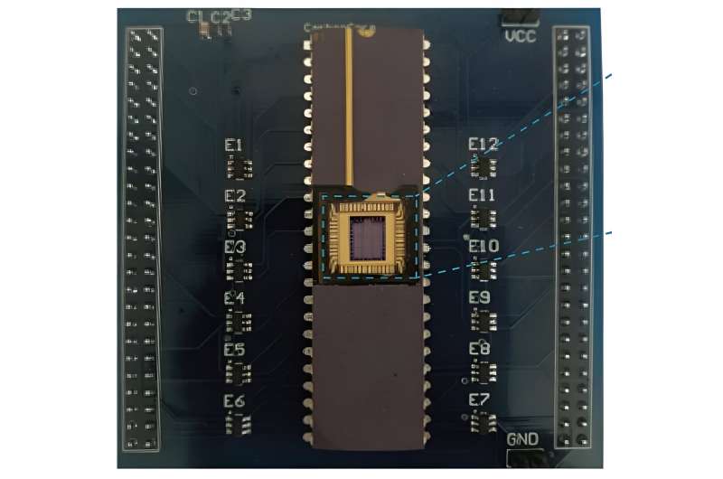
Researchers at Peking University and other institutes in China recently developed a highly promising tensor processing unit (TPU) based on carbon nanotubes that could be used to run AI algorithms more energy-efficiently. This carbon nanotube-based tensor processing chip, presented in a paper in Nature Electronics, could be a key breakthrough on the path towards developing next-generation chips.
“We successfully developed the world’s first tensor processor chip (TPU) based on carbon nanotubes,” Zhiyong Zhang, co-author of the paper, told Tech Xplore. “We were inspired by the fast development of AI applications as well as TPU by Google. From ChatGPT to Sora, artificial intelligence is ushering in a new revolution, but traditional silicon-based semiconductor technology is increasingly unable to meet the processing needs of massive amounts of data. We have found a solution in the face of this global challenge.”
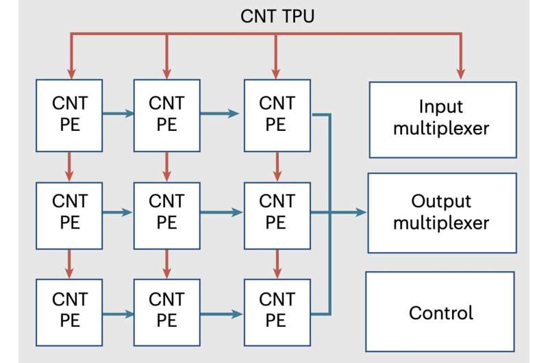
In computer science, systolic arrays are networks of processors that rhythmically compute data and allow it to pass through them freely, similar to how blood flows through the human body. Zhang and his colleagues developed a new efficient systolic array architecture using carbon nanotube transistors, field effect transistors (FETs) with channels made of carbon nanotubes instead of conventional semiconductors. Building on this new architecture they developed, they created the world’s first carbon-nanotube-based TPU reported to date.
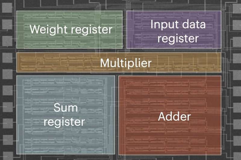
“The chip is composed of 3,000 carbon nanotube field-effect transistors, organized as 3*3 processing units (PEs),” Zhang explained. “These 9 PEs form a systolic array architecture, which can perform two-bit integer convolution and matrix multiplication operations in parallel.”

The tightly coupled architecture introduced by Zhang and his colleagues supports the flow of systolic input data. This flow of data through the architecture reduces read and write operations of static random-access memory (SRAM) components, which translates into significant energy savings.
“Each PE receives the data from its upstream neighbors (up and left), independently calculates a partial result within itself, and passes it downstream (right and down),” Zhang said. “Each PE is designed for 2-bit MACs and matrix multiplication on signed and unsigned integers. Combined with systolic data flow, the CNT TPU could accelerate convolution operations in NN applications.”
The team’s proposed system architecture was carefully designed to accelerate tensor operations performed by artificial neural networks, easily switching between integer convolutions and matrix multiplications. The tensor processing chip they developed based on this architecture could be a crucial milestone for the development of new, high-performing integrated circuits based on low-dimensional electronics.
“Based on our carbon-based tensor processor chip, we built a five-layer convolutional neural network that can perform image recognition tasks with an accuracy rate of up to 88% and a power consumption of only 295μW, which is the lowest power consumption among all new convolutional acceleration hardware technologies,” Zhang said.
“The system simulation results show that the carbon-based transistor using the 180 nm technology node can reach 850 MHz and the energy efficiency exceeds 1TOPS/w, which shows obvious advantages over other device technologies at the same technology node.”

Overall, the results of initial simulations and tests performed by the researchers highlight the potential of their carbon-based TPU, suggesting that it may be well-suited for running machine learning-based computational models. In the future, their chip could display greater computing power and be more energy-efficient than existing devices based on semiconductors.
This research team’s efforts could eventually help accelerate the operations of convolutional neural networks while reducing their power consumption. In the meantime, Zhang and his colleagues plan to further increase the performance, energy efficiency and scalability of their chip.
“The performance and energy efficiency of this approach could be further enhanced by, for example, using aligned semiconducting CNTs as channel materials, reducing the transistor size, increasing the bits of PEs, or implementing CMOS logic,” Zhang added.
“The CNT TPU could also potentially be built in BEOL in a silicon fab for three-dimensional integration: that is, a silicon CPU at the bottom with a CNT TPU on top as a co-processor. Moreover, 3D monolithic integration of multilayer CNT FETs could be studied for potential advantages of reduced latency and more bandwidth.”
More information: Jia Si et al, A carbon-nanotube-based tensor processing unit, Nature Electronics (2024). DOI: 10.1038/s41928-024-01211-2.
Journal information: Nature Electronics

Leave a Reply