August 13, 2024 by Danielle Roedel, Brookhaven National Laboratory
Collected at: https://phys.org/news/2024-08-sources-energy-loss-quantum-gains.html
Scientists from Yale University and the U.S. Department of Energy’s (DOE) Brookhaven National Laboratory have developed a systematic approach to understanding how energy is lost from the materials that make up qubits. Energy loss inhibits the performance of these quantum computer building blocks, so determining its sources—and adjusting the materials as necessary—can help bring researchers closer to designing quantum computers that could revolutionize several scientific fields.
With their new approach, the Yale scientists were able to design a compact device that could store quantum information for more than one millisecond.
This research, published in Nature Communications, was conducted as part of the Co-Design Center for Quantum Advantage (C2QA), a national quantum information science research center led by Brookhaven Lab. Yale is a key partner of the center.
“A significant hurdle that we must overcome is improving the ability of qubits to retain the quantum information encoded in them. This is known as coherence,” explained Suhas Ganjam, who is first author of the new paper. Ganjam conducted the research as a doctoral student at Yale and is now a research scientist at Google.
A few years ago, Princeton University researchers—who joined C2QA upon its establishment —designed qubits with a record-breaking coherence time of 0.3 milliseconds by replacing the traditionally used niobium or aluminum with a superconducting metal called tantalum. This indicated that qubits’ constituent materials directly affect their performance, but the reasons for this were still unclear.
So, scientists contributing to C2QA began investigating the different kinds of tantalum oxides that form on tantalum’s surface when it is exposed to air. They further improved coherence by coating tantalum with a thin layer of magnesium that prevented the material’s oxidation.
“Researchers have been building devices with better coherence times. But there are so many different sources of energy loss, and we still couldn’t distinguish which ones were improving,” said Ganjam. “So, we set out to differentiate between the different types of loss.”
Under the supervision of Robert Schoelkopf, a physicist at Yale University who leads the Devices Thrust of C2QA, Ganjam designed a device called a tripole stripline.
This new device consists of three superconducting thin-film strips patterned on a substrate, similar to other quantum devices. The strips were arranged in a special way so that the researchers could not only quantify energy lost but also determine where it was being lost by testing the device in three different modes—one for each pair of superconducting electrodes.
For example, the researchers could differentiate between surface loss and bulk dielectric loss by observing modes in which electromagnetic fields were either confined to the surface of the device or spread throughout the substrate. If they observed more loss from the mode in which electromagnetic fields were confined to the surface of the device, the loss was dominated by the surface contribution.
“Through our electromagnetic tests with the tripole stripline, we could observe that devices made with tantalum and aluminum lose different amounts of energy in different ways,” Ganjam explained.
In particular, the researchers found that using a tantalum thin film, rather than an aluminum thin film, reduced surface loss. And using a fabrication technique called annealing, which involves heating a sapphire substrate and letting it cool slowly, reduced the bulk dielectric loss.
“We wanted to know why the different materials and fabrication techniques influenced loss like this,” Ganjam said. “So, we turned to our collaborators from the Center for Functional Nanomaterials.”
Quantum materials through the microscopy lens
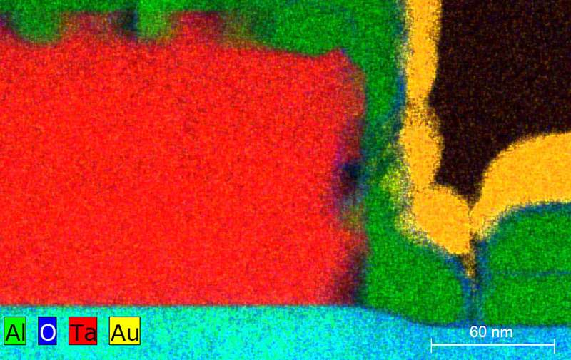
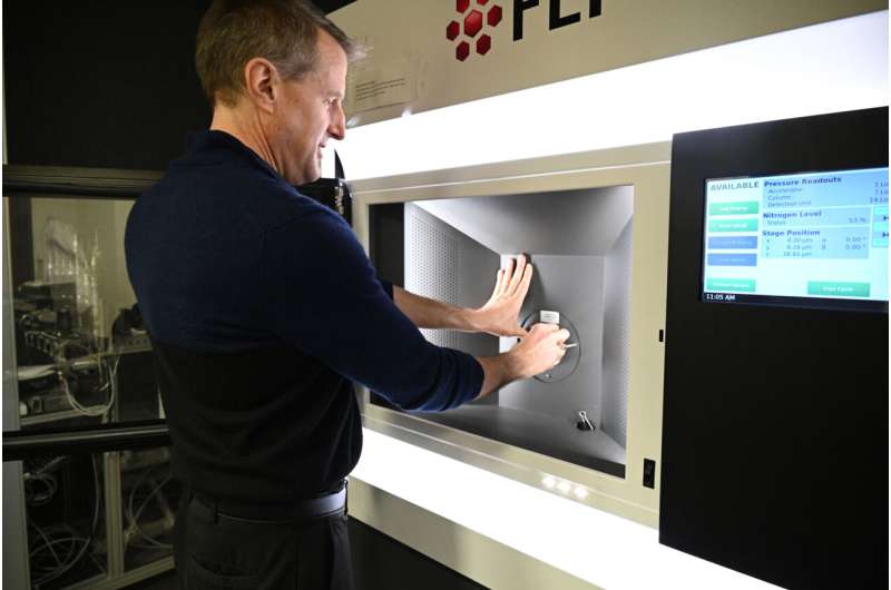
The Center for Functional Nanomaterials (CFN) is a DOE Office of Science user facility at Brookhaven Lab with a state-of-the-art Electron Microscopy facility. Using transmission electron microscopy and scanning transmission electron microscopy to look at the materials’ microscopic structure, scientists from this facility can help other researchers, like Ganjam and Schoelkopf, better understand the materials they are working with.
“We suspect that qubit coherence is limited by energy loss that is due to contaminants or defects in the materials,” explained Minghzao Liu, a senior scientist at CFN. “So, we analyze the quantum materials at CFN to look for these coherence-limiting characteristics.”
Kim Kisslinger, an advanced technical associate at CFN, extracted microscopic cross-sections of the Yale scientists’ materials and devices and analyzed them at the atomic level.
“I view projects like this through an electron microscopy lens,” said Kisslinger. “From crystallinity to chemical composition to epitaxy, which is related to the orientation of the crystal materials, I can tell our collaborators exactly what is going on with their materials and help them correlate these properties with the materials’ performance.”

Liu said, “Kim helps our collaborators better understand their materials, but he also helps them make meaningful improvements through an iterative process.”
Kisslinger added, “CFN is home to cutting-edge equipment that can support the materials research needed for quantum devices. But we also have some of the most qualified scientists and specialists in the world. This combination of quality people and quality equipment is unique to CFN.”
Collaborative efforts yield improved devices
With a well-rounded understanding of the electromagnetic properties of their devices, as well as the material composition, the Yale researchers utilized an energy loss model that could predict a device’s coherence based on its constituent materials and the circuit geometry. And with the help of this predictive model, they optimized circuit geometry to build a quantum device with a coherence time greater than one millisecond.
“This research marks an important milestone in the C2QA mission. Even beyond the longer coherence time, it demonstrates a path forward to further coherence enhancements through the close collaboration of quantum device and materials scientists,” said C2QA Deputy Director Kai-Mei Fu.
The collaboration between the qubit design experts from the Schoelkopf lab and CFN materials characterization experts, which began with the establishment of the center, embodies C2QA’s principle of “co-designing” materials and algorithms to achieve quantum computers that outperform classical computers.
“Collaborations like this one are key to unlocking the best materials and optimal fabrication processes that will help C2QA realize their goal,” Ganjam said.
“It has been quite rewarding to see these qubit design projects grow in scope and success over the years,” added Liu. “Scientific advances like this are not possible without collaboration.”
More information: Suhas Ganjam et al, Surpassing millisecond coherence in on chip superconducting quantum memories by optimizing materials and circuit design, Nature Communications (2024). DOI: 10.1038/s41467-024-47857-6
Journal information: Nature Communications

Leave a Reply