July 29, 2024 by National University of Singapore
Collected at: https://techxplore.com/news/2024-07-technique-fabricate-dimensional-circuits-advanced.html
Unlike traditionally printed circuit boards, which are flat, 3D circuitry enables components to be stacked and integrated vertically—dramatically reducing the footprint required for devices.
Advancing the frontiers of 3D printed circuits, a team of researchers from the National University of Singapore (NUS) has developed a state-of-the-art technique—known as tension-driven CHARM3D—to fabricate three-dimensional (3D), self-healing electronic circuits. This new technique enables the 3D printing of free-standing metallic structures without requiring support materials and external pressure.
The research team led by Associate Professor Benjamin Tee from the Department of Materials Science and Engineering in the NUS College of Design and Engineering used Field’s metal to demonstrate how CHARM3D can fabricate a wide range of electronics, allowing for more compact designs in devices such as wearable sensors, wireless communication systems and electromagnetic metamaterials.
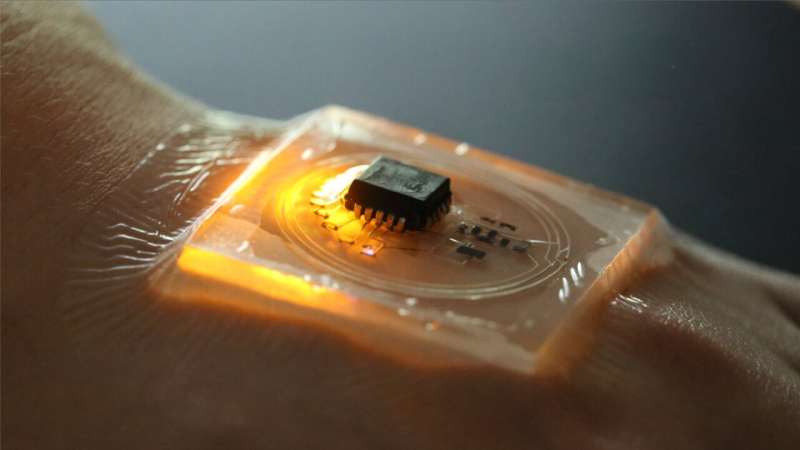
In health care, for instance, CHARM3D facilitates the development of contactless vital sign monitoring devices—enhancing patient comfort while enabling continuous monitoring. In signal sensing, it optimizes the performance of 3D antennas, leading to improved communication systems, more accurate medical imaging and robust security applications.
The team’s findings were published in the journal Nature Electronics on 25 July 2024. Assoc Prof Tee is the corresponding author of the research paper.
A more streamlined approach to 3D circuit manufacturing
3D electronic circuits increasingly underpin modern electronics, from battery technology to robotics to sensors, enhancing their functionalities while enabling further miniaturization. For example, 3D architectures, with their large effective surface areas, improve battery capacity and enhance sensor sensitivity.
Direct ink writing (DIW), a promising 3D printing technique currently used to fabricate 3D circuits, poses significant drawbacks. The crux lies in its use of composite inks, which have low electrical conductivity and entail support materials to aid in solidification after printing. The inks are also too viscous, limiting printing speed.
Enter Field’s metal, an eutectic alloy of indium, bismuth and tin. Eutectic alloys melt and freeze at a single temperature lower than the melting points of their constituent metals—offering an attractive alternative material for 3D printing. With a low melting point of 62°C, a high electrical conductivity and low toxicity, Field’s metal, unlike composite inks, solidifies rapidly—a crucial characteristic that enables the printing process to eschew support materials and external pressure.
Leveraging the low melting point of Field’s metal, the CHARM3D technique exploits the tension between molten metal in a nozzle and the leading edge of the printed part, culminating in uniform, smooth microwire structures with adjustable widths of 100 to 300 microns, roughly the width of one to three strands of human hair. Critically, phenomena such as beading and uneven surfaces—characteristic of pressure-driven DIW—are also absent in CHARM3D.
Compared to conventional DIW, CHARM3D offers faster printing speeds of up to 100 millimeters per second and higher resolutions, offering a greater level of detail and accuracy in circuit fabrication. CHARM3D forgoes post-treatment steps and enables the fabrication of complex free-standing 3D structures, such as vertical letters, cubic frameworks and scalable helixes. Moreover, these 3D architectures exhibit excellent structural retention with self-healing capabilities, meaning they can automatically recover from mechanical damage and are recyclable.
“By offering a faster and simpler approach to 3D metal printing as a solution for advanced electronic circuit manufacturing, CHARM3D holds immense promise for the industrial-scale production and widespread adoption of intricate 3D electronic circuits,” said Assoc Prof Tee.

Far-reaching applications
The researchers successfully printed a 3D circuit for wearable battery-free temperature sensors, antennas for wireless vital sign monitoring and metamaterials for electromagnetic wave manipulation—capturing the diversity of applications enabled by CHARM3D.
Traditional hospital equipment such as electrocardiograms and pulse oximeters require skin contact, which can cause discomfort and risk infections. Through CHARM3D, contact-free sensors can be integrated into smart clothing and antennas, providing continuous, accurate health monitoring in hospitals, assisted-living facilities or home settings.
Furthermore, arrays of 3D antennas or electromagnetic metamaterial sensors—fabricated via CHARM3D—could optimize signal sensing and processing applications. This leads to improved signal-to-noise ratios and higher bandwidths. The technique opens up the possibility of creating specialized antennas for targeted communication, enabling more accurate medical imaging, such as microwave breast imaging for early tumor detection, and advanced security applications, such as detecting hidden devices or contraband emitting specific electromagnetic signatures.
Other collaborators in this work include Dr. Zhuangjian Liu from Agency for Science, Technology and Research’s Institute of High Performance Computing and Professor Michael Dickey from North Carolina State University’s Department of Chemical and Biomolecular Engineering.
Next steps
The research team envisions that this technique can be extended to other types of metals and structural applications. The team is also looking for opportunities to commercialize this unique approach to metal printing.
More information: Shaohua Ling et al, Tension-driven three-dimensional printing of free-standing Field’s metal structures, Nature Electronics (2024). DOI: 10.1038/s41928-024-01207-y
Journal information: Nature Electronics

Leave a Reply