By Ashwini Sakharkar 25 Jul, 2024
Collected at: https://www.techexplorist.com/caltechs-nanoscale-device-reflect-direct-light-desired-ways/86497/
Imagine a future where every individual has access to lightning-fast, dedicated wireless channels for communication that are hundreds of times faster than today’s Wi-Fi. Thanks to the groundbreaking development of metasurfaces – tiny engineered sheets that can reflect and otherwise direct light in desired ways, this may soon become a reality.
A team of Caltech engineers revealed a metasurface embedded with miniscule tunable antennas capable of reflecting optical light to generate multiple sidebands or channels of varying optical frequencies. This advancement has the potential to revolutionize communication and connectivity as we know it.
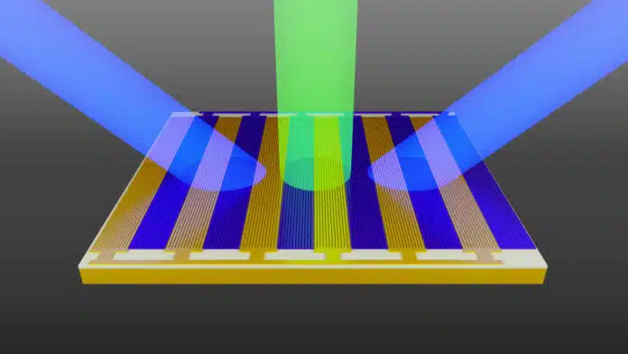
“With these metasurfaces, we’ve been able to show that one beam of light comes in, and multiple beams of light go out, each with different optical frequencies and going in different directions,” says Harry Atwater, the Otis Booth Leadership Chair of the Division of Engineering and Applied Science, the Howard Hughes Professor of Applied Physics and Materials Science, and senior author on the new paper. “It’s acting like an entire array of communication channels. And we’ve found a way to do this for free-space signals rather than signals carried on an optical fiber.”
The research presents a groundbreaking approach for not only creating a new form of wireless communication channel, but also potentially developing innovative range-finding technologies and a novel method for relaying large amounts of data to and from space.
Prachi Thureja, a co-lead author of the new paper and a graduate student in Atwater’s group, explains that to comprehend their work, it’s important to first understand the term “metasurface.” The prefix “meta” is derived from Greek, meaning “beyond.”
Metasurfaces are designed to surpass the capabilities of traditional bulky optical elements, like camera or microscope lenses. These multi-layer transistor-like devices are engineered with a carefully selected pattern of nanoscale antennas that can manipulate light through reflection, scattering, and other control methods. These flat devices can both focus and reflect light, similar to a lens or mirror, through the strategic design of an array of nanoscale elements that modify the behavior of light.
Atwater’s group has paved the way for a new era in metasurface technology by focusing on active metasurfaces rather than passive ones. In their latest breakthrough, they have developed a space-time metasurface capable of dynamically directing light at specific frequencies, operating at optical frequencies commonly used in telecommunications. This revolutionary device, measuring just 120 microns wide and long, holds the potential to significantly enhance available bandwidth at optical frequencies.
At radio frequencies, electronic devices can proficiently manipulate the direction of light beams, a capability commonly employed in radar navigation systems for aircraft. However, at higher optical frequencies, there is a lack of electronic devices that can achieve this. Therefore, the researchers opted for a different approach by modifying the properties of the antennas themselves.
Jared Sisler, a co-lead author on the paper, and Thureja developed a metasurface consisting of gold antennas with an electrically tunable semiconductor layer of indium tin oxide. Through the application of a specific voltage profile, they can locally adjust the density of electrons in the semiconductor layer beneath each antenna, thereby altering its refractive index and light-bending properties.
“By having the spatial configuration of different voltages across the device, we can then redirect the reflected light at specified angles in real-time without the need to swap out any bulky components,” Thureja says.
“We have an incident laser hitting our metasurface at a certain frequency, and we modulate the antennas in time with a high-frequency voltage signal. This generates multiple new frequencies, or sidebands, that are carried by the incident laser light and can be used as high-data-rate channels for sending information. On top of this, we still have spatial control, meaning we can choose where each channel goes in space,” explains Sisler. “We are generating frequencies and steering them in space. That’s the space-time component of this metasurface.”
The team’s groundbreaking work showcases the capability of a metasurface to split and redirect light at optical frequencies in free space, offering potential applications in LiDAR technology. This light-based equivalent of radar can capture depth information from a three-dimensional scene.
The team’s vision is to craft a “universal metasurface” that can generate multiple optical channels, each carrying information in different directions in free space.
“If optical metasurfaces become a realizable technology that proliferates, a decade from now, you’ll be able to sit in a Starbucks with a bunch of other people on their laptops, and instead of each person getting a radio frequency Wi-Fi signal, they will get their own high-fidelity light beam signal,” says Atwater, who is also the director of the Liquid Sunlight Alliance at Caltech. “One metasurface will be able to beam a different frequency to each person.”
The team is partnering with JPL’s Optical Communications Laboratory, a pioneer in utilizing optical frequencies for space communication. This revolutionary approach allows for transmitting significantly larger volumes of data at higher frequencies. “These devices would be perfect for what they’re doing,” says Sisler.
Journal reference:
- Jared Sisler, Prachi Thureja, Meir Y. Grajower, Ruzan Sokhoyan, Ivy Huang & Harry A. Atwater. Electrically tunable space–time metasurfaces at optical frequencies. Nature Nanotechnology, 2024; DOI: 10.1038/s41565-024-01728-9
Leave a Reply