JULY 18, 2024 by Patsy DeLacey, University of Michigan
Collected at: https://techxplore.com/news/2024-07-optogpt-solar-cells-smart-windows.html
Solar cell, telescope and other optical component manufacturers may be able to design better devices more quickly with AI. OptoGPT, developed by University of Michigan engineers, harnesses the computer architecture underpinning ChatGPT to work backward from desired optical properties to the material structure that can provide them. The paper is published in the journal Opto-Electronic Advances.
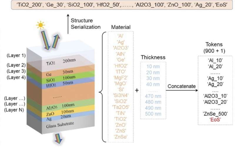
The new algorithm designs optical multilayer film structures—stacked thin layers of different materials—that can serve a variety of purposes. Well-designed multilayer structures can maximize light absorption in a solar cell or optimize reflection in a telescope. They can improve semiconductor manufacturing with extreme UV light, and make buildings better at regulating heat with smart windows that become more transparent or more reflective depending on temperature.
OptoGPT produces designs for multilayer film structures within 0.1 seconds, almost instantaneously. In addition, OptoGPT’s designs contain six fewer layers on average compared to previous models, meaning its designs are easier to manufacture.
“Designing these structures usually requires extensive training and expertise as identifying the best combination of materials, and the thickness of each layer, is not an easy task,” said L. Jay Guo, U-M professor of electrical and computer engineering and corresponding author of the study.
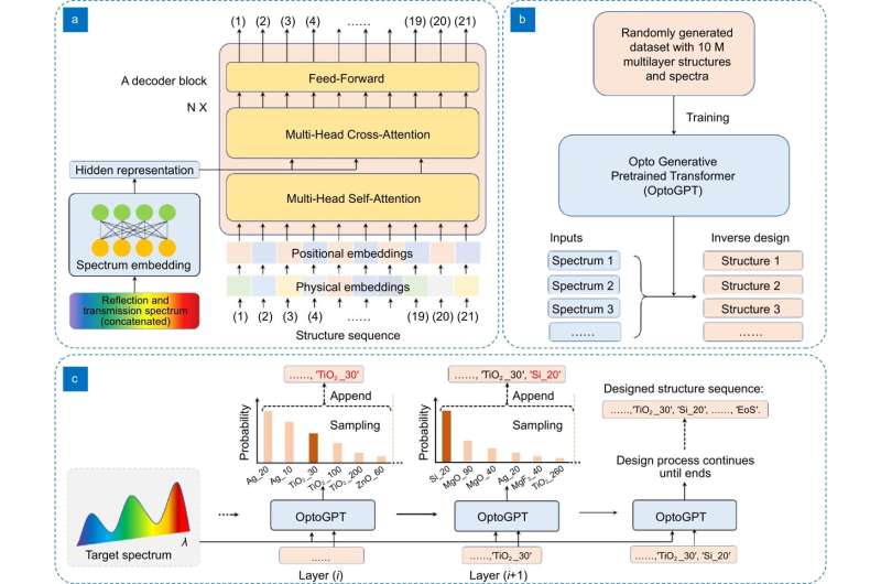
For someone new to the field, it’s difficult to know where to start. To automate the design process for optical structures, the research team tailored a transformer architecture—the machine learning framework used in large language models like OpenAI’s ChatGPT and Google’s Bard—for their own purposes.
“In a sense, we created artificial sentences to fit the existing model structure,” Guo said.
The model treats materials at a certain thickness as words, also encoding their associated optical properties as inputs. Seeking out correlations between these “words,” the model predicts the next word to create a “phrase”—in this case a design for an optical multilayer film structure—that achieves the desired property such as high reflection.

Researchers tested the new model’s performance using a validation dataset containing 1,000 known design structures including their material composition, thickness and optical properties. When comparing OptoGPT’s designs to the validation set, the difference between the two was only 2.58%, lower than the closest optical properties in the training dataset at 2.96%.
Similar to how large language models are able to respond to any text-based question, OptoGPT is trained on a large amount of data and able to respond well to general optical design tasks across the field.
If researchers are focused on a task, like designing a high-efficiency coating for radiative cooling, they can use local optimization—adjusting variables within bounds to achieve the best possible outcome—to further fine-tune the thickness to improve accuracy. During testing, the researchers found fine-tuning improves accuracy by 24%, reducing the difference between the validation dataset and OptoGPT responses to 1.92%.
Taking the analysis a step further, the researchers used a statistical technique to map out associations that OptoGPT makes.
“The high-dimensional data structure of neural networks is a hidden space, too abstract to understand. We tried to poke a hole in the black box to see what was going on,” Guo said.
When mapped in a 2D space, materials cluster by type such as metals and dielectric materials, which are electrically insulating but can support an internal electric field. All dielectrics, including semiconductors, converge upon a central point as the thickness approaches 10 nanometers. From an optics perspective, the pattern makes sense as light behaves similarly regardless of material as they approach such small thicknesses, helping further validate OptoGPT’s accuracy.
Known as an inverse design algorithm because it starts with the desired effect and works backward to a material design, OptoGPT offers more flexibility than previous inverse design algorithm approaches, which were developed for specific tasks. It enables researchers and engineers to design optical multilayer film structures for a wide breadth of applications.
Additional co-authors include Taigao Ma and Haozhu Wang of the University of Michigan.
More information: Taigao Ma et al, OptoGPT: A foundation model for inverse design in optical multilayer thin film structures, Opto-Electronic Advances (2024). DOI: 10.29026/oea.2024.240062

Leave a Reply