JULY 17, 2024 by Michael Matz, Lawrence Berkeley National Laboratory
Collected at: https://phys.org/news/2024-07-approach-discovery-quantum-materials.html
Researchers at the Department of Energy’s Lawrence Berkeley National Laboratory (Berkeley Lab) and several collaborating institutions have successfully demonstrated an innovative approach to find breakthrough materials for quantum applications. The study is published in the journal Nature Communications.
The approach uses rapid computing methods to predict the properties of hundreds of materials, identifying short lists of the most promising ones. Then, precise fabrication methods are used to make the short-list materials and further evaluate their properties.
The study team included researchers at Dartmouth College, Penn State, Université Catholique de Louvain (UCLouvain), and University of California, Merced.
“In our approach, theoretical screening guides the targeted use of atomic-scale fabrication,” said Alex Weber-Bargioni, one of the study’s principal investigators and a scientist at Berkeley Lab’s Molecular Foundry, where much of this research was conducted.
“Together, these methods open the door for researchers to accelerate the discovery of quantum materials with specific functionalities that can revolutionize computing, telecommunications, and sensors.”
The promise of light-sensitive quantum defects
Quantum information science involves the use of atomic-scale phenomena to encode, process, and transmit information. One way to achieve this control is to create defects in materials—such as replacing one type of atom with another. These defects can be incorporated into systems that enable quantum applications.
“For defects to work for quantum applications, they need to have very specific electronic properties and structures,” said Geoffroy Hautier, a Dartmouth materials scientist and the project’s lead investigator. “They should preferably be able to absorb and emit light with wavelengths in the visible or telecommunications range.”
Two-dimensional (2D) materials—which are just one atom or molecule thick—are prime candidates to host such high-performance quantum defects due to their unique electronic properties and tunability.
Finding a needle in a haystack
There’s a catch, however. Defects with good quantum properties are very difficult to find.
“Consider the material tungsten disulfide (WS2),” said Sinéad Griffin, a Berkeley Lab scientist and one of the study’s principal investigators.
“If you account for the dozens of periodic table elements that could be inserted into this material and all the possible atomic locations for the insertion, there are hundreds of possible defects that could be made. Looking beyond WS2, if you consider thousands of possible materials for defects, there are literally infinite possibilities.”
Functional quantum defects are typically discovered by accident. The traditional approach is for experimentalists to fabricate and evaluate defects one at a time. If one defect doesn’t have good properties, they repeat the process for another one.
When a good one is finally found, theorists investigate why its properties are good. Exploring the hundreds of possible defects for WS2 in this manner would take several decades.
The study team flipped this traditional approach, starting with theory and finishing with experiments. The basic idea: use theoretical computation as a guide to identify a much smaller number of promising defects for experimentalists to fabricate.

Hautier, Griffin, and postdoctoral researchers Yihuang Xiong (Dartmouth) and Wei Chen (UCLouvain) developed state-of-the-art, high-throughput computational methods to screen and accurately predict the properties of more than 750 defects in 2D WS2. The defects involved substituting a tungsten or sulfur atom with one of 57 other elements. The calculations were designed to identify defects with an optimal set of properties related to stability, electronic structure, and light absorption and emission.
The massive number of calculations, based on quantum mechanics principles, took advantage of the high performance computing resources at the National Energy Research Scientific Computing Center (NERSC) at Berkeley Lab. The analysis identified one defect—made by substituting a sulfur atom with a cobalt atom—with particularly good quantum properties. Before the study, no defect in WS2 was known to have these properties.
In addition to the traditional publication format, the team is sharing the results of its search with the global research community in a publicly available database called the Quantum Defect Genome. The researchers started the database with WS2 and have extended it to other host materials such as silicon. The aim is to encourage other researchers to contribute their data and build a large database of defects and their properties for various host materials.
Playing with atoms like LEGO bricks
The next step was for experimentalists to fabricate and examine this cobalt defect. Such a task has historically been challenged by a lack of control over where defects form in materials. But Berkeley Lab researchers found a solution. Working at the Molecular Foundry, the team developed and applied a technique that enables atomic-level precision in fabrication.
Here’s how it worked: A 2D WS2 sample in a super-low-temperature vacuum was heated, and its surface was blasted with argon ions at just the right angle and energy. This caused a small fraction of the sulfur atoms to pop out, leaving tiny holes in the material.
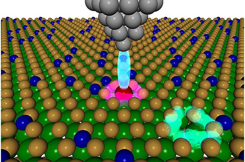
A mist of cobalt atoms was applied on the surface. The sharp metal tip of a scanning tunneling microscope was used to find a hole and nudge a cobalt atom into it—similar to putting in golf. Finally, the researchers used the microscope’s tip to measure the electronic properties of the cobalt defect.
“The microscope’s tip can see individual atoms and push them around,” said John Thomas, a Berkeley Lab postdoctoral researcher who conducted the fabrication.
“It allows us to select a specific location for the cobalt atom and match the structure of the defect identified in the computational analysis. We’re essentially playing with atoms like LEGO bricks.”
Importantly, this method enables fabrication of identical defects. This is necessary for defects to interact with each other in quantum applications—a phenomenon known as entanglement. In quantum communications, for instance, one possible application is for defects to transmit information across a long-distance fiber-optic cable through light emission and absorption.
Experimental confirmation of theoretical predictions
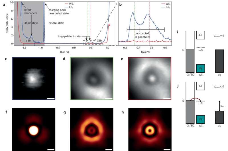
The experimental measurements of the defect’s electronic structure agreed with the computational predictions, demonstrating the accuracy of the predictions.
“This critical result shows the effectiveness of combining our computation and fabrication approaches to identify defects with sought-after properties,” said Weber-Bargioni.
“It points to the value of using these approaches in the future.”
“Many factors came together to make this study a success,” said Hautier. “In addition to the computation and fabrication methods, our secret sauce was how the theorists and experimentalists collaborated. We met regularly and gave each other constant feedback on our methods to optimize the overall study. This deep collaboration was enabled by having common funding for the entire team.”
The team’s next step is to make additional measurements on the cobalt defect’s properties and investigate how to improve them. The researchers also plan to use their computational and fabrication methods to identify other high-performance defects. For example, desirable quantum states are fragile and can be easily disturbed by tiny vibrations that occur naturally in materials. It may be possible to engineer defects that are shielded from these vibrations.
“The ability to build complex materials with atomic precision—driven by theory—allows us to highly optimize their properties and potentially discover material functionalities that we do not even have a name for today,” said Weber-Bargioni. “We have built ourselves a huge materials playground for us to play in.”
More information: John C. Thomas et al, A substitutional quantum defect in WS2 discovered by high-throughput computational screening and fabricated by site-selective STM manipulation, Nature Communications (2024). DOI: 10.1038/s41467-024-47876-3
Journal information: Nature Communications

Leave a Reply