
JUNE 13, 2024 by Optica
Collected at: https://techxplore.com/news/2024-06-photonic-chip-ultrafast-machine-vision.html
Researchers have demonstrated a new intelligent photonic sensing-computing chip that can process, transmit and reconstruct images of a scene within nanoseconds. This advance opens the door to extremely high-speed image processing that could benefit edge intelligence for machine vision applications such as autonomous driving, industrial inspection and robotic vision.
Edge computing, which performs intensive computing tasks like image processing and analysis on local devices, is evolving into edge intelligence by adding artificial intelligence (AI) driven analysis and decision-making.
“Capturing, processing and analyzing images for edge-based tasks such as autonomous driving is currently limited to millisecond-level speeds due to the necessity of optical-to-electronic conversions,” said research team leader Lu Fang from Tsinghua University in China.
“Our new chip can perform all these processes in just nanoseconds by keeping them all in the optical domain. This could be used to significantly enhance, or even replace, the traditional architecture of sensor acquisition followed by AI post-processing.”
In Optica the researchers describe the new chip, which they call an optical parallel computational array (OPCA) chip. They show that the OPCA has a processing bandwidth of up to one hundred billion pixels and a response time of just 6 nanoseconds, which is about six orders of magnitude faster than current methods. They also used the chip to create an optical neural network that integrates image perception, computation and reconstruction.
“The chip and optical neural network could boost the efficiency of processing complex scenes in industrial inspection and help advance intelligent robot technology to a higher level of cognitive intelligence,” said Wei Wu, co-first author of the paper. “We think it could also revolutionize edge intelligence.”
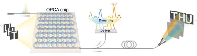
The new intelligent optical computational array (OPCA) chip performs end-to-end image processing, transmission and reconstruction by integrating sensing and computing on one chip. Credit: Wei Wu, Tsinghua University
Eliminating optical to electrical conversions
Machine vision—which uses cameras, image sensors, lighting and computer algorithms to capture, process and analyze images for specific tasks—traditionally involves converting optical information into digital electrical signals using sensors. These signals are then transmitted over optical fibers for long-distance data transmission and downstream tasks.
However, the frequent conversion between optical and electrical signals along with limited advancements in electronic processors has become a major restriction on improving the speed and processing capacity of machine vision.
“The world is entering an AI era, but AI is very time- and energy-exhaustive,” said Fang. “Meanwhile, the growth of edge devices, such as smartphones, intelligent cars and laptops has resulted in explosive growth of image data to be processed, transmitted and displayed. We are working to advance machine vision by integrating sensing and computing in the optical domain, which is particularly important for edge computing and for enabling more sustainable AI applications.”
The challenge in performing both image acquisition and analysis on the same chip in the optical domain is finding a way to convert the free-space spatial light used for imaging into an on-chip guided light wave.
More information: Wei Wu et al, A parallel photonic chip for nano-second end-to-end image processing, transmission, and reconstruction, Optica(2024). DOI: 10.1364/OPTICA.516241. opg.optica.org/optica/abstract … 0.1364/OPTICA.516241
Journal information: Optica
Leave a Reply